X-ray inspection technology isn’t just limited to the medical domain; it is also used by various manufacturing companies, especially in the tech sector. X-ray inspection used in the tech sector is commonly referred to as ‘Automated X-ray Inspection.’ It’s the process of inspecting the concealed features of target products or components with X-rays. Countless tech manufacturing fields such as aerospace, electronics, industrial control, etc., apply X-ray inspection technology, particularly for inspecting PCB boards.
Since PCBs are fundamental to most of the equipment or devices manufactured in these sectors, testing their quality is a must. That’s why the use of X-ray inspection in PCB assembly processes is extremely common. As a result, the leading PCB manufacturers of the world prefer to employ soldering professionals who can conduct these tests and adapt their soldering skills as per the revelations of these tests.
Table of Contents
Why X-Ray Testing is So Popular in Electronics Manufacturing
The electronics manufacturing industry is by far the most active and profitable manufacturing sector in the world. The American electronics manufacturing industry itself is worth over $300 billion. Hence, leading soldering professionals look for jobs in this sector. Electronic X-ray inspection and sorting are skills that are highly acclaimed in this sector because X-ray copies of solder joints can be examined automatically to spot structural defects. Soldering professionals with these skills can save a ton of their employers’ time and money with these skills.
Defects such as insufficient solder, shorts, voiding, etc., on average, make up 80%-90% of all the overall defects on assembled circuit boards. These common defects can be spotted and corrected on the spot by a soldering professional who knows how to conduct X-ray testing and sort their design processes accordingly. Since the electronics manufacturing industry has become tremendously sophisticated in the last few decades, there’s no room for such structural defects or inconsistencies anymore.
The electronics industry constantly partners with industrial, military, and aerospace industries, and small errors could lead to compliance issues. Hence, leading electronics manufacturing companies prioritize hiring soldering professionals who have received extensive training in this field.
Why X-Ray Testing Skills are Vital for All Soldering Professionals
Not only has the electronics manufacturing industry become more sophisticated, but the products coming out of this sector have also become extremely sophisticated and hard to inspect as well. Modern-day soldering or welding professionals must know about electronic X-ray sorting because –
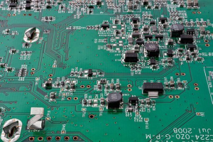
Smaller Components – Electrical equipment is becoming more compact and more layered every year. All equipment manufacturers are aiming to minimize space and maximize functionality in their products. The solder joints and components in such small electronic equipment are placed in extremely complex manners. They are now being placed in internal layers in very complicated and intricate ways. For instance, a solder joint might be placed in-between multiple PCB layers. Or, they may need to be hidden somewhere inside the final product. Detecting such intricately placed solder joints is impossible with the naked eye. Hence, soldering professionals have to use their X-ray testing skills to detect these concealed solder joints and micro-components.
PCB Miniaturization – On average, the sizes of circuit board components have become extremely smaller over the last few years. To make up for the small-sized components, PCB manufacturers are creating denser boards. Hence, thermal, optical, or ultrasonic imaging methods are ineffective as modern-day PCBs are super-dense. X-ray inspection is the only inspection method that can collect comprehensive images of these super-dense boards. In the future, PCB manufacturers aim to create denser boards. So, the use of X-ray inspection methods is here to stay.
The Rise of Surface Mount Technology (SMT) – Most devices and equipment coming out of American electronics manufacturing industries are surface-mount. That means they were manufactured using surface-mount technology. In this method, electrical components are installed or mounted directly on PCB surfaces. While SMT does make electronic devices smaller and manufacturing processes much simpler, they also require super-dense PCBs. Thin PCBs won’t be able to handle the pressure of direct mounting. That’s why soldering professionals need to use X-ray inspection methods to detect the presence of micro-components concealed between layers.
X-Ray Testing – A Must-Know Skill
Traditional inspection methods to detect defects in PCBs don’t work anymore. Only X-rays can penetrate the dense layers of PCBs and allow soldering professionals to inspect their inner layers. More importantly, X-ray technology allows soldering professionals to inspect the solder joints of multifaceted PCB assemblies. In 2019, the median pay for soldiering professionals was $42,490 per year (or $20.43 per hour). Soldering professionals who are adept at X-ray sorting are likelier to earn much more since their demand in the electronics manufacturing sector is much higher. A soldering professional who has mastered X-ray inspection equipment can detect PCB boards defects such as –
- Missing Components
- Solder Joints
- Inadequate Solder
- Substandard Soldering
- Poor Bridging,
- Solder Joints on The Board
Soldering professionals must receive training in the field of electronic x-ray sorting and inspection of super-dense printed circuit boards to advance their chances of securing higher-paying jobs.