The exponential growth in the electronics market has increased the demand for Printed Circuit Boards or PCBs. PCB is a flat, rigid, insulating material, and it is the foundational building block of most modern electronic devices. It consists of lines and pads that connect various points. It allows signals and power to be routed between physical devices. Conductive pathways are etched or “printed” onto the circuit board, which connects various components like transistors, resistors, and integrated circuits.
Over the last few years, a quiet revolution has happened in Turnkey PCB Assembly. The global PCB market is expected to reach an estimated $89.7 billion by 2024 with a CAGR of 4.3% from 2019 to 2024. This has increased the pressure on original equipment manufacturers (or OEMs) to build adaptable and sustainable boards. PCB fabrication and assembly process involves the soldering of components upon the bare board.
The circuit board comprises a substrate made of fibreglass, a copper layer, and holes in which the components are fitted. A PCB can be either single-sided or double-sided. The PCB substrate is insulated with a solder mask to prevent short circuits, and epoxy resin holds it together.
Table of Contents
6 Basic Things You Should Know About PCB Assembly Process
· Solder Paste
Before you fit the components, you need to apply the solder paste to the required areas. You can do this by using solder paste to the stainless steel stencil. A mechanical fixture holds the stencil and PCB together. You can apply the solder paste evenly with the applicator’s help. Hence the right amount of solder paste needs to be used. It ensures that the correct volume goes into the resulting joints. When you remove the applicator, the solder paste remains in the desired area of the PCB. Solder paste is minute solder grains laced with flux.
· Placement of Components
The second step in the PCB assembly process or PCBA is the automated placement of surface mount components on the PCB board. The components are mounted directly onto a printed circuit board’s surface with a pick and place machine. It takes the components from the dispenser and places them in the desired location on the circuit board. The designer creates a file that is fed to the automated robot to perform the required operation. The components are placed on the solder paste, and the tension from the solder paste keeps the pieces intact.
To secure the components on the board, some pick and place machines add glue drops. In this soldering process, degradable glue is the best option to avoid repair complications. Before the automated machines came into use, technicians will use tweezers to place the components on PCB. However, this was an exhausting process, and automated pick and place machines have made the task much more accessible. These robots can place the components accurately and work 24/7 without fatigue.
· Reflow Soldering
After the solder paste is applied and necessary components are placed rightly on the PCB, you need to pass the board through a soldering machine for reflow soldering. In this process, PCBs and the soldered components are put on the conveyer belt. The conveyer belt moves the PCBs and the components in a giant oven with a temperature of 250°C. The solder melts, secures the components upon the PCB, and creates joints. The PCB is cooled down to solidify the components in a controlled manner to create a permanent joint between mounted components and PCB. In double-sided PCBs, the side with fewer or smaller components is applied with solder paste to place the components before the side, which will have more components.
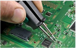
· QC and Inspection
After the completion of soldering, PCBs should be inspected for any misalignment or other errors.
- Manual Inspection: It can be used for boards that use the through-hole technology method. However, visually testing the printed circuit boards can result in fatigue and eye strain. It cannot be used for PCBs which use the SMT method to mount small components.
- Optical Inspection: It uses an automated machine with high-powered and high-resolution cameras installed at various angles. These machines are used to inspect solder joints from different directions. Automated Optical Inspection (AOI) machine operates at very high speed.
- X-ray Inspection: It is used to inspect inner layer defects. It is only used for advanced and complex PCBs.
· Testing
Before the electronic product is packaged, it needs to be tested thoroughly. A functionality test should be performed to check that the PCB gives a seamless performance. PCB is supplied with electrical signals and power at specified pins and output. The functioning of PCB is checked at these specified test points and output connectors.
You need to visually inspect the PCB to check that the components are in place. Verify current, voltage, analog, and digital signals across two areas of the circuit and electrical components. You can also perform in-circuit testing to check various parameters like frequency and voltage.
· Final Cleaning, Finishing, and Shipment
After you test your PCB comprehensively to check for any loopholes, you have to clean the unwanted residual flux, finger dirt, and oil stains on the board. You can use a stainless steel-based high-pressure washing tool that uses deionized water to clean the PCB. Dry it with compressed air after washing it. Your PCB is ready for packaging and shipment.
To Conclude:
Printed circuit board assembly involves building a surface mount technology (SMT) board using pick and place techniques. PCB assembly deploys several individual stages, and each step flows into the next to build a high-quality PCB.